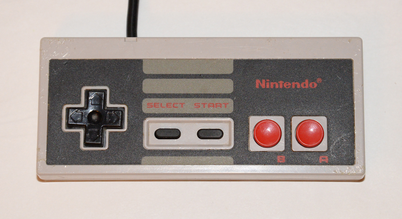
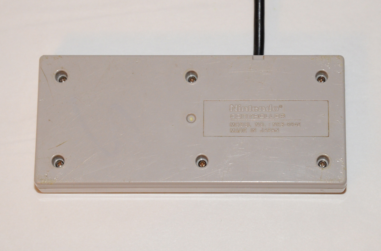
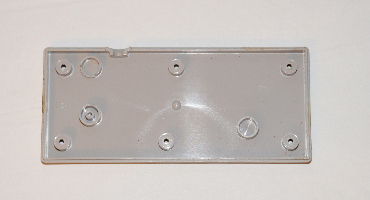
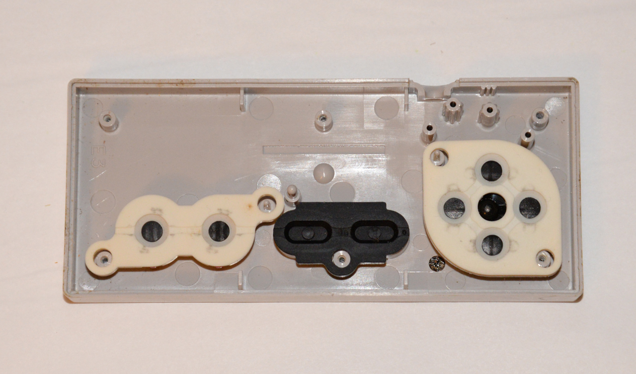
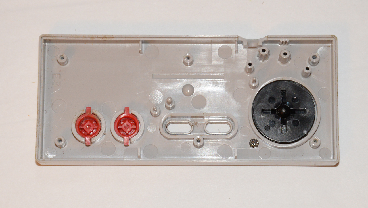
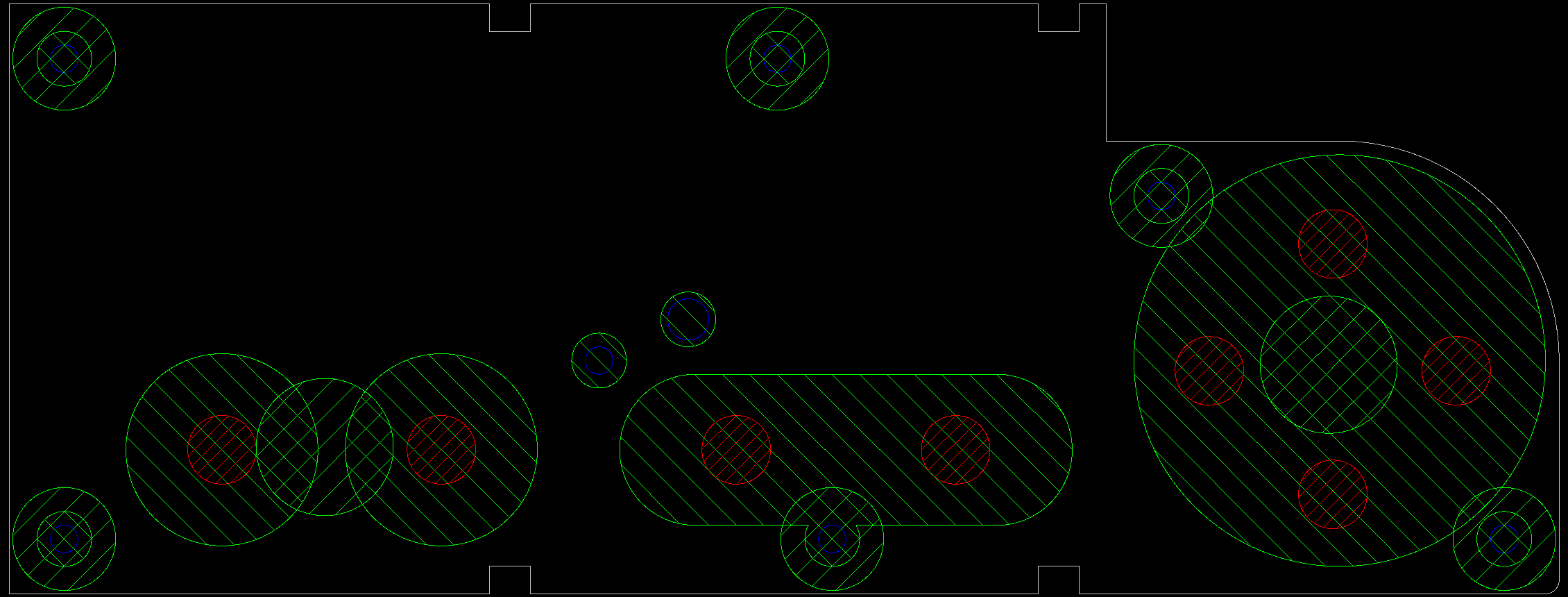
I am working on modifying a NES gamepad. I took me some time to take the dimensions of the PCB and the keepout area where the mounts are in the controller. I’m posting the dimensions here so maybe it saves you some time.
And remember, the dimensions are not guaranteed to be correct. If you find a mistake, drop me a note.
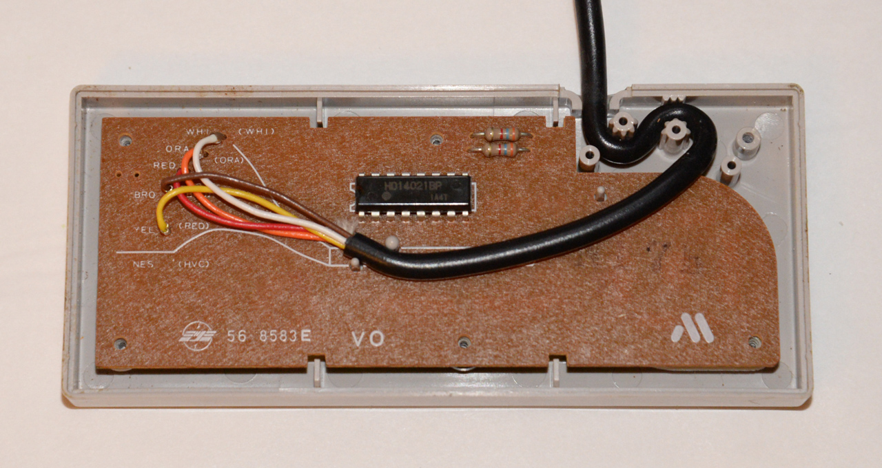
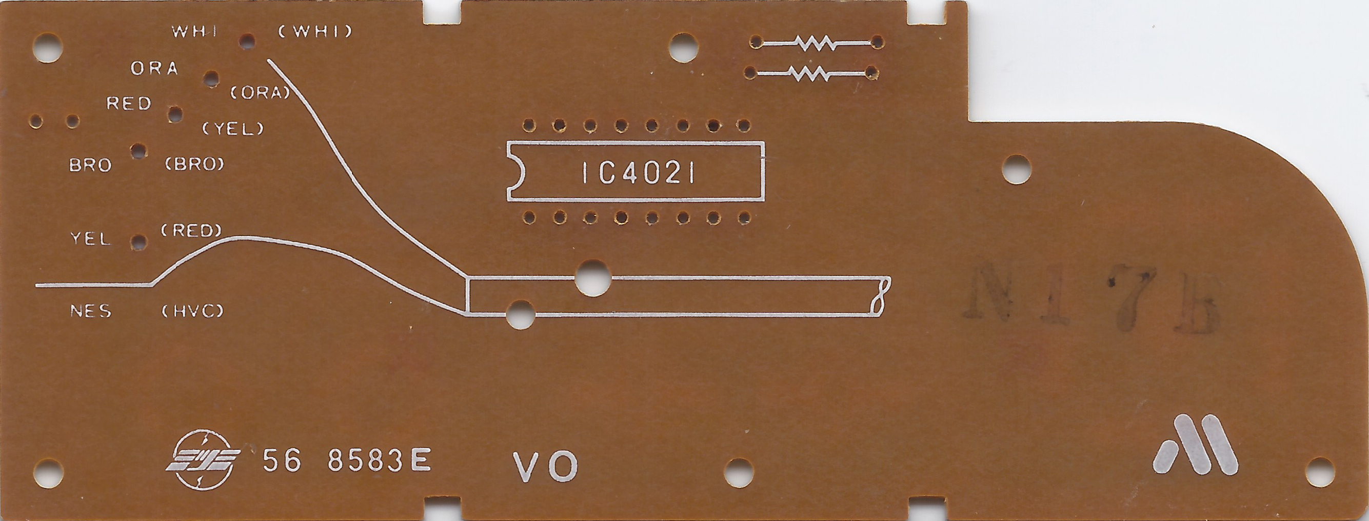
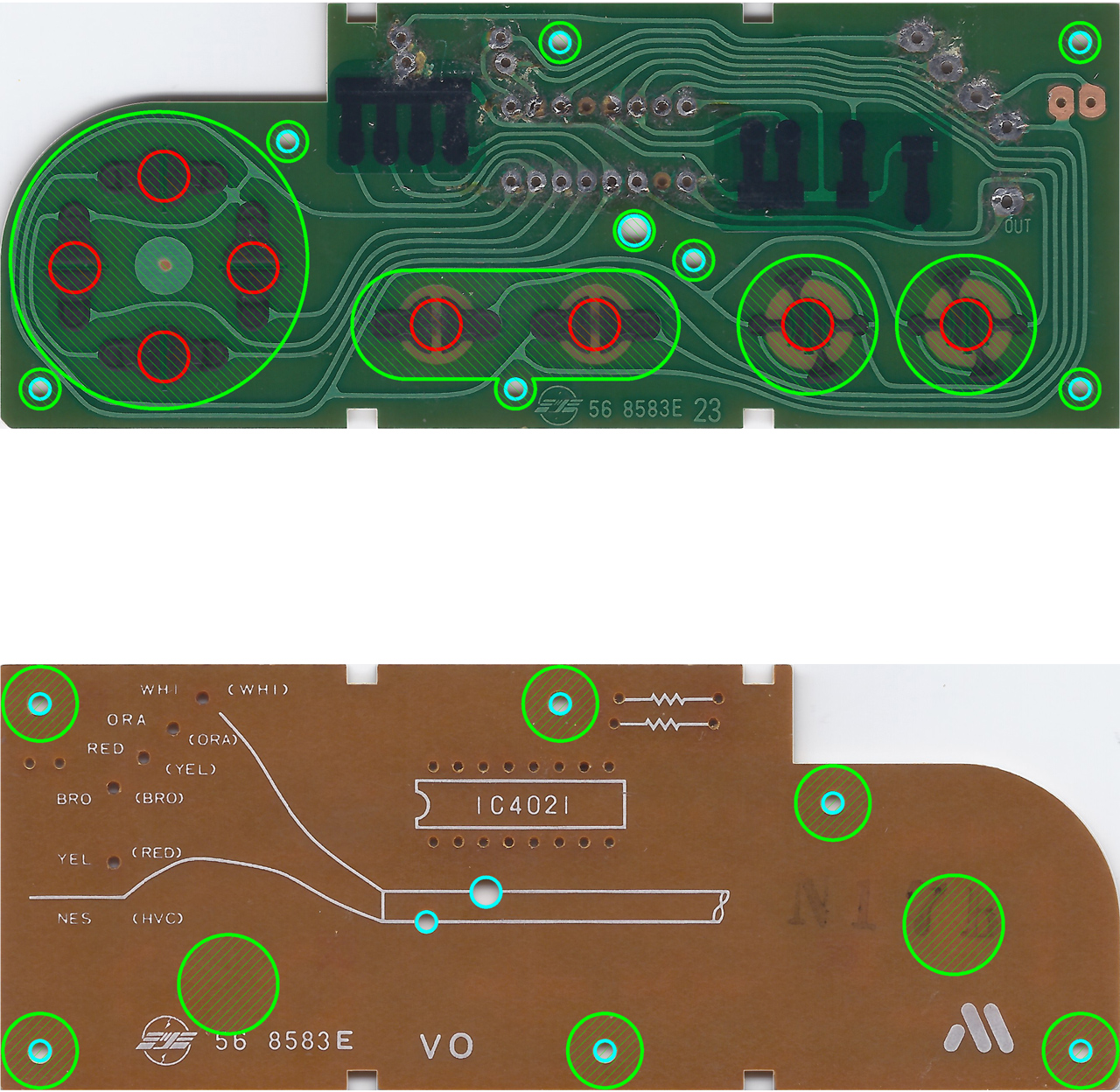
IC4021 is an 8-bit shift register with parallel inputs and serial output. It is clocked by the NES. Both resistors are 3.6k Ohm
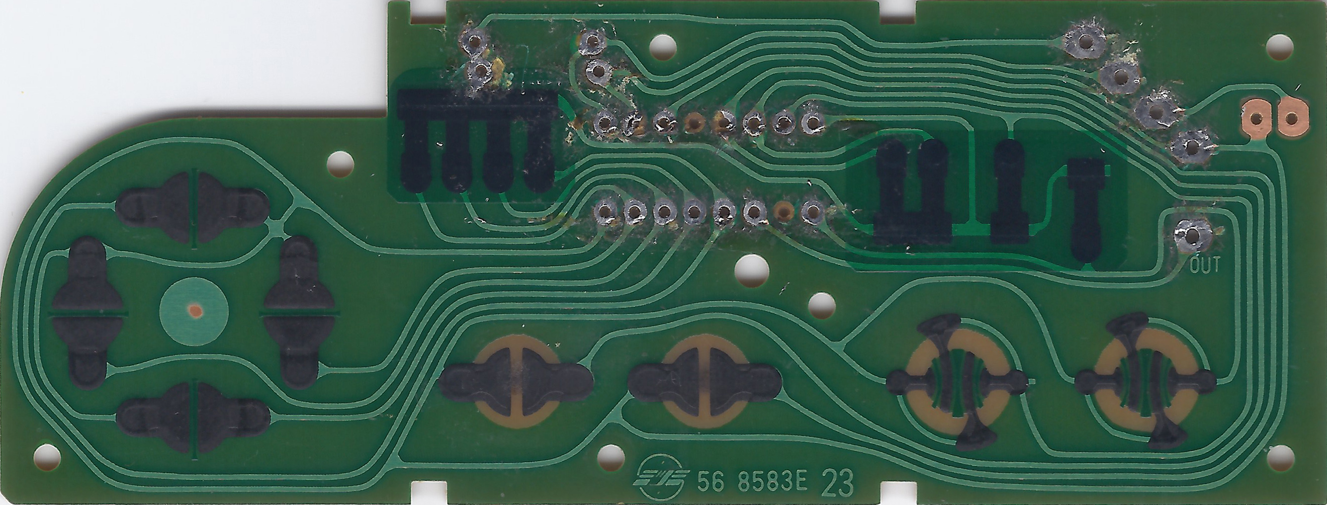
Please note that the eight pull-up resistors printed direct to the pcb. They are located to the left and to the right of the solder pads of the shift register. Their value is roughly 50k Ohm.
Download link (use: Save link as)
You’re my hero dude! Great DFX. Imports into Catia wonderfully. Im making a PCB from this, so I’ll put your name on it too.
Did you ever make a PCB from the DXF file? It would be nice to make a replacement board.
Glad to hear you could make use of it.
Have you managed to make a pcb that we could print and solder an alternative to IC4021 to?